A single contact material can efficiently deliver charge into two distinct kinds of atomically thin semiconductors, researchers report, signalling a possible route to smaller and more energy‑efficient AI chips. A team led by KAIST has developed a van der Waals tunnelling injector made from tin diselenide (SnSe2) that works with both monolayer p‑type tungsten diselenide (WSe2) and monolayer n‑type molybdenum disulphide (MoS2).
What the team built
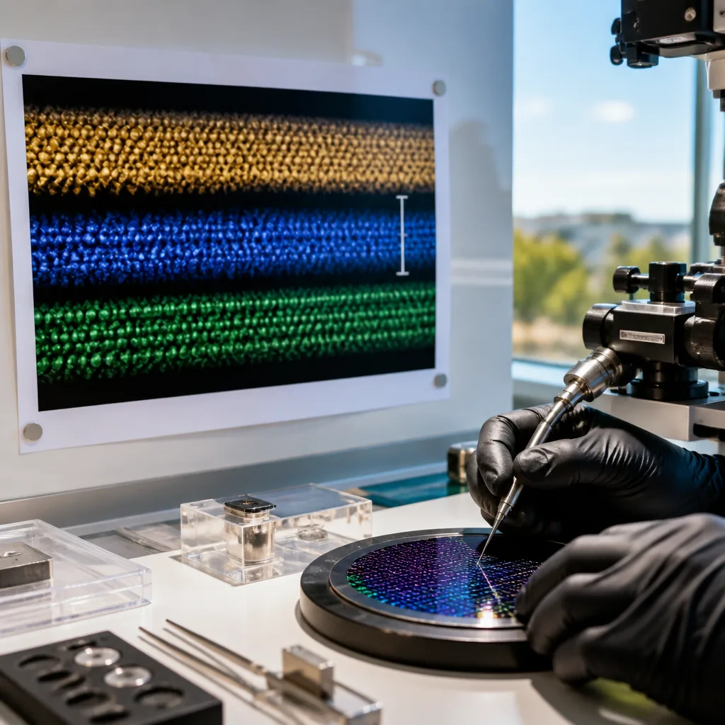
The group engineered an injector that interfaces with ultrathin semiconductor channels without heavy chemical bonding, using weak van der Waals forces to preserve atomically clean contacts. Electron microscopy showed an atomically sharp SnSe2–MoS2 interface with an interlayer spacing of about 2.15 Å. Surface potential mapping indicated the SnSe2 contact was more uniform than a conventional, directly deposited nickel contact, an important practical advantage for device reproducibility.
Why this matters
Transistors in modern chips rely on efficient injection of charge carriers. In n‑type devices electrons carry current; in p‑type devices the current is carried by holes (the absence of an electron). Historically, contacts have been separately engineered for n‑ and p‑type materials because the required energy alignments differ. The KAIST approach uses one contact material to provide different energy alignments to each monolayer semiconductor, allowing a single fabrication step to serve both transistor types in vertically stacked, ultrathin devices.
- Simplicity: One injector material replaces separately optimised contacts for n‑ and p‑type layers.
- Scalability: Atomically thin contacts are compatible with vertical integration of multiple layers to boost device density.
- Uniformity: Surface potential mapping found the SnSe2 contact to be more uniform than deposited nickel, which can reduce device variation.
How it works — a brief technical primer
The device relies on two concepts. First, van der Waals contacts avoid creating disruptive chemical bonds at the interface, keeping the semiconductor’s atomic lattice intact. Second, a tunnelling injector supplies carriers across a thin barrier by quantum tunnelling, rather than by forming a conventional metallic contact that pins energy levels. Together these features let the same injector present different effective energy barriers to different semiconducting monolayers, enabling both electron and hole injection from one material.
| Material | Role | Observed property |
|---|---|---|
| SnSe2 | Universal van der Waals tunnelling injector | Uniform surface potential; atomically sharp interfaces |
| WSe2 (monolayer) | p‑type channel (holes) | Receives hole injection |
| MoS2 (monolayer) | n‑type channel (electrons) | Interface spacing ≈ 2.15 Å |
Collaboration and context
The work was led by Professor Joonki Suh’s team at KAIST and involved collaborators at Yonsei University, the Beijing Computational Science Research Center, KIST, Hanyang University, UNIST and Samsung Electronics. The researchers frame the development as a potential enabler for next‑generation AI and low‑power semiconductor devices where multiple ultrathin layers are stacked to increase device density and performance.
While the reported findings are promising, they are an intermediate step. Demonstrating a reliable laboratory contact that supplies carriers to two monolayer materials does not immediately translate to mass‑manufactured silicon‑complementary processes. Engineering challenges remain around large‑area growth, integration with existing foundry flows and long‑term stability under operating conditions.
Nonetheless, the result addresses a long‑standing practical problem in two‑dimensional electronics — how to make contacts that do not destroy the atomic quality of the channel and that can be applied uniformly at scale. By using a van der Waals tunnelling mechanism, the injector avoids some pitfalls of direct metal deposition such as damage to ultrathin layers and uncontrolled Fermi‑level pinning.
For South Africa and other countries seeking to participate in the global semiconductor ecosystem, advances that reduce process complexity and increase device density could be important. A universal injector material could decrease the number of process steps and bespoke materials needed to fabricate advanced two‑dimensional devices, potentially lowering barriers to entry for specialised chip lines focused on low‑power AI acceleration.
These findings illustrate a broader trend in materials science: combining precision structural characterisation with device engineering to solve interface problems at the atomic scale. If follow‑on work confirms manufacturability and reliability, the SnSe2 injector approach may influence how future ultrathin transistors are realised.