Penn State researchers have built a prototype memory device that integrates synthetic DNA with a crystalline perovskite semiconductor, creating a bio-hybrid component that stores and processes information at very low energy levels. The work, published in Advanced Functional Materials and the subject of a patent application, suggests a possible route to more power-efficient computing platforms and data storage.
Bridging biology and electronics
The team capitalised on two complementary properties: the extraordinary information density of DNA and the strong electronic behaviour of perovskite materials already used in solar cells and some data technologies. A single gram of DNA, the researchers note, can encode an immense amount of data — about 215 million gigabytes — making it an attractive medium for dense storage if its chemistry can be made compatible with conventional electronics.
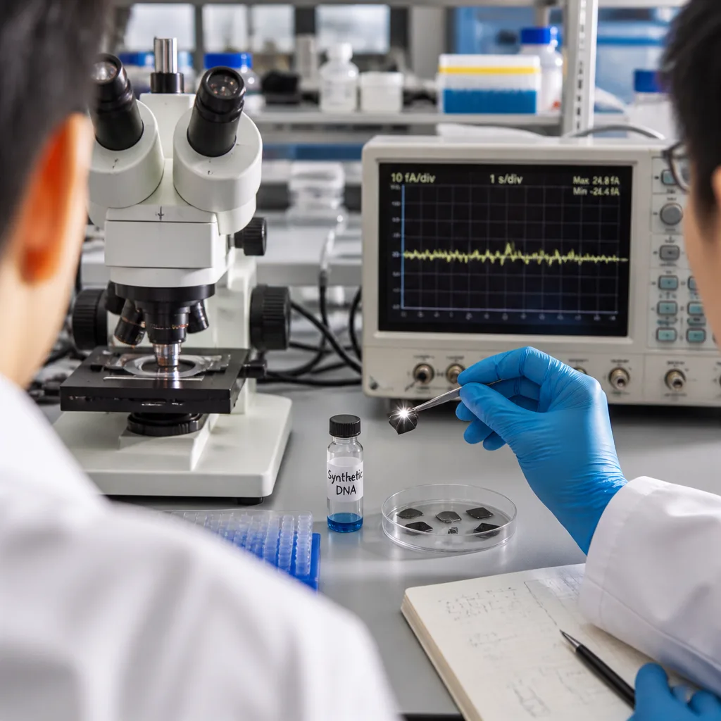
To overcome the long-standing incompatibility between biological molecules and solid-state electronic materials, the group designed short, chemically synthesised DNA sequences tuned to the needs of an electronic device. Those synthetic strands were paired with a crystalline perovskite semiconductor to create a memory resistor, commonly known as a memristor.
"Biology and electronics are different domains. Bridging these two fields required developing an entirely new materials platform that allows them to function seamlessly together," said Kavya S. Keremane, co-corresponding author and postdoctoral researcher in materials science and engineering at Penn State.
Memristors differ from ordinary resistors because they can retain a record of prior electrical activity — effectively remembering past current flow even after power is removed. That property enables storage and computation to occur in the same physical location, a point of interest for researchers seeking architectures that mimic neural processing.
Device architecture and potential
The published work describes a device architecture where the engineered DNA interfaces with the perovskite layer to produce non-volatile memory behaviour while operating with very low energy input. The authors contend this bio-hybrid approach fundamentally changes how low-power memory devices can be designed.
Although the research is at an early stage, the combination of high-density molecular information storage and a semiconductor backbone could offer advantages in several areas:
- Lower energy consumption for memory operations, relevant to energy-hungry data centres and training of artificial intelligence systems.
- Co-located storage and processing, reducing the need to shuttle data between separate memory and compute units — a known bottleneck in existing architectures.
- High density potential by leveraging DNA’s compact information encoding capabilities.
| Component | Role |
|---|---|
| Synthetic DNA | Information-bearing medium engineered into short sequences for electronic compatibility |
| Perovskite semiconductor | Electronic host material providing charge transport and stability |
| Memristor device | Non-volatile memory element combining both materials to store and process signals |
The research team emphasises that the work required an entirely new materials platform to let the biological and electronic components operate together without degrading one another. The effort included tailoring molecular chemistry and device processing steps so that the DNA-based elements could coexist with crystalline perovskite layers under conditions needed for stable electronic function.
Context and next steps
DNA has long been recognised for its data density, and recent years have seen growing interest in molecular and biomolecular approaches to storage. Perovskite semiconductors likewise have attracted attention for their tunable electronic properties and ease of fabrication. Combining the two addresses several limitations that have kept biological macromolecules largely separate from conventional device engineering.
The report is a proof-of-concept and the researchers have filed a patent application. Key questions that remain include the device longevity under operational cycling, large-scale manufacturability, environmental stability, and the precise energy and speed metrics when compared with incumbent memory technologies. Those technical benchmarks will determine whether the approach can move from laboratory demonstrations to commercial or infrastructure applications.
If the approach matures, the implications extend beyond denser archives: memory that can store and compute simultaneously could help mitigate the escalating energy demands of data centres and certain AI workloads by reducing data movement and operating at lower voltages.
The marriage of a biologically inspired information carrier and conventional semiconductor physics illustrates a broader trend in materials science: hybrid solutions that exploit strengths from disparate domains to solve scaling and efficiency challenges in computing.