Extremely small, sharply curved wrinkles in graphene can produce substantial electrical charge separation, researchers report, offering experimental proof that geometry alone can reshape electronic behaviour in atom-thin materials.
The team, working at Rice University and publishing their findings in Advanced Materials, used high-resolution probes and spectroscopic techniques to map tiny bends in single-layer carbon and measure local electrical energy and current. Their results provide direct evidence for flexoelectricity — an effect where uneven bending generates an electric charge — in graphene, a material just one atom thick.
How a wrinkle acts like a microscopic battery
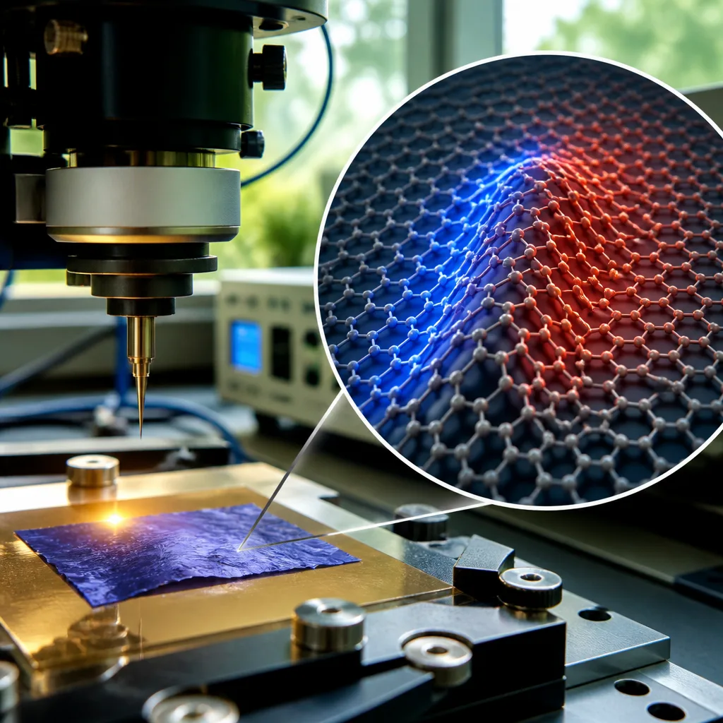
Graphene is a flat lattice of carbon atoms. The researchers focused on wrinkles that form naturally in the sheet. When a bend is squeezed into a region smaller than a nanometre, the intense curvature causes electrons to displace slightly to one side of the sheet, producing two opposite electrical faces akin to the poles of a tiny battery.
"Our work shows that even an ordinary wrinkle can become an extraordinary electronic feature when viewed at the atomic scale,"
The remark came from Pulickel Ajayan, co-corresponding author and professor of engineering at Rice. Lead author Sathvik Ajay Iyengar, a former doctoral student, used the ruler analogy to explain the scale: the bend is like flexing a flexible ruler, but confined to a space far smaller than a billionth of a metre, provoking a measurable electron shift.
Methods and measurements
To link shape and electrical response the team combined several experimental approaches. They employed specialised microscope probes capable of resolving the shape of individual wrinkles while simultaneously measuring local electrical energy and current. Raman spectroscopy — a laser technique sensitive to atomic-scale strain — was used to quantify how atoms were stretched or compressed. Computational simulations complemented the measurements to interpret how curvature produced the observed charge separation.
| Technique | Purpose |
|---|---|
| High-resolution probe microscopy | Map wrinkle geometry and local electrical signals |
| Raman spectroscopy | Detect atomic strain (stretching/compression) |
| Computer simulations | Interpret link between curvature and electron distribution |
The combination of direct measurement and modelling enabled the authors to attribute the local charge separation to flexoelectric effects rather than chemical changes or material contamination.
Implications and next steps
By demonstrating that simple geometry can control electronic behaviour in a two-dimensional material, the study points to an alternative design principle for ultrathin devices: tune the shape at the atomic scale rather than alter chemistry or layer composition. Potential applications include more sensitive sensors and extremely thin electronic components in which local electrical properties are defined by engineered curvature.
Practical exploitation will require reliable ways to create and stabilise the required sub-nanometre curvature and to integrate these features into device architectures. The research is an early step that shows the effect exists and can be measured; moving from laboratory demonstration to manufacturing remains a challenge.
Key aspects that future work may address include:
- Methods to fabricate and pattern controlled wrinkles at sub-nanometre scale.
- Stability of flexoelectric charge under operating conditions and over time.
- Integration strategies for device-scale electronics that exploit geometry-driven properties.
One clear attraction of the approach is conceptual simplicity: engineers could design devices whose functionality derives from shape, much as macroscopic mechanical devices rely on geometry. At the atomic scale, this result suggests a new lever for materials design where curvature becomes a tool as powerful as doping or stacking.
While the work focuses on graphene, flexoelectricity is a general phenomenon and might be sought in other two-dimensional materials, expanding the palette for future nanoscale electronic design.