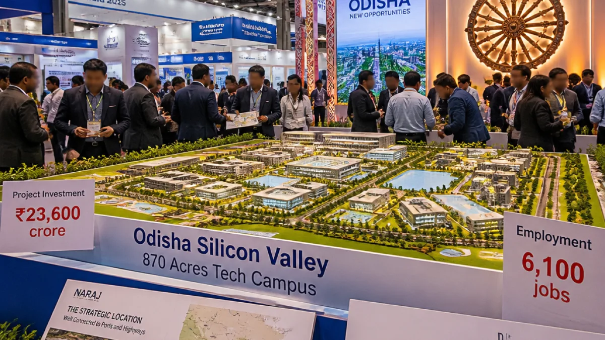
Bhubaneswar: The Odisha government on Friday announced plans to develop an 870-acre technology and semiconductor hub — branded as the Odisha Silicon Valley — at Naraj near Cuttack, aiming to attract large-scale semiconductor, electronics and IT manufacturing under a wider push mapped out at SEMICON India 2026 in New Delhi.
Big-ticket proposals at SEMICON India
Chief Minister Mohan Charan Majhi unveiled the plan while inaugurating the Odisha pavilion at the industry event, where the state recorded investment proposals totalling approximately ₹23,600 crore. The proposals, according to the state, have the potential to create roughly 6,100 direct jobs.
Majhi described the Naraj site as strategically located with “seamless connectivity to the Cuttack-Bhubaneswar urban corridor, multimodal access to the ports of Paradip and Dhamra and links to key national highways,” saying these factors make the location attractive for the semiconductor supply chain, logistics and allied industries.
“Odisha is steadily building the foundation to become Eastern India’s Silicon Valley... Discussions with industry leaders were focused on taking this momentum forward and bringing the next set of semiconductor investments to Odisha,” said Mohan Charan Majhi.
Industry engagement and signed intents
During the event the chief minister held meetings with global and domestic semiconductor and technology firms and international delegations, including groups from Japan, Sweden and Taiwan. Companies reportedly engaged in discussions included Lam Research, Applied Materials, SiCSem, 3D Glass Solutions, Cyient, Linde and HORIBA India.
The state government also signed a letter of intent with QuadQuantum for a facility to manufacture silicon carbide (SiC) substrate wafers — a component used in power electronics and advanced semiconductor devices. The Odisha pavilion showcased projects and initiatives involving RIR Power, SiCSem, 3D Glass Solutions and ARF Design, the state said.
Site advantages and requirements
Officials emphasised the Naraj location's industrial advantages cited at the event: connectivity to major ports and highways and proximity to the Mahanadi River, which could support industrial water requirements for fabrication, assembly and related units. The package was positioned as supportive of India Semiconductor Mission 2.0 and the state's broader aim to host critical parts of the semiconductor value chain.
While the announcement underlines investment interest, successful execution typically requires parallel investments in power, water, skilled manpower, land clearance and environmental safeguards. Representatives at SEMICON India discussed both manufacturing prospects and the need to build an ecosystem that allows global and Indian technology companies to manufacture, innovate and grow in Odisha.
- Site: 870 acres at Naraj, near Cuttack
- Investment proposals: ~₹23,600 crore
- Potential jobs: ~6,100
- Key engagements: Delegations from Japan, Sweden, Taiwan; companies including Lam Research and Applied Materials
- LoI: QuadQuantum for SiC substrate wafer facility
How this could affect Odisha
If projects move from proposals to implementation, the Naraj hub could diversify Odisha’s industrial base beyond traditional sectors and strengthen the eastern corridor as a technology manufacturing cluster. The project would also tie into existing logistics networks through Paradip and Dhamra ports and the Cuttack-Bhubaneswar corridor.
Officials and industry players at the event emphasised that building a semiconductor-ready ecosystem takes time and sustained policy, including land allotment, infrastructure provisioning and workforce development. The state’s ability to translate the present interest into signed agreements and executed projects will be the next measure of progress.
| Item | Details |
|---|---|
| Planned area | 870 acres (Naraj) |
| Investment proposals | Approximately ₹23,600 crore |
| Potential employment | About 6,100 jobs |
| Notable engagement | LoI with QuadQuantum (SiC wafer facility) |
Practical considerations for residents and policymakers
For local communities and policy planners, the focus will need to be on balanced development — ensuring employment and economic benefits while addressing environmental and civic infrastructure needs. Key considerations include:
- Ensuring reliable power and industrial water without compromising local supplies.
- Advance planning for road, rail and port connectivity to handle cargo and personnel movement.
- Skilling initiatives so local youth can access new job opportunities in manufacturing and services.
- Strict environmental clearances and pollution control measures for semiconductor-relevant industries.
The announcement marks a significant step in Odisha’s push to be an eastern hub for high-technology manufacturing. The state administration’s next tasks will be to convert the proposals into firm investment agreements and to begin preparatory work on land, infrastructure and regulatory clearances that such projects require.
Reporting from New Delhi; further updates expected as companies formalise investments and site-level plans are revealed.