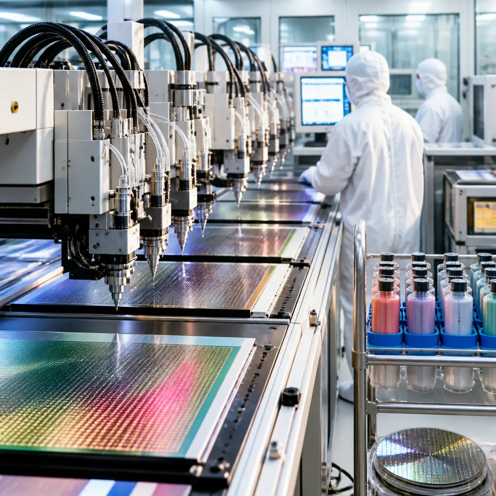
Manz Asia and SUSS have announced a collaboration to accelerate the use of inkjet printing in semiconductor manufacturing and advanced packaging, with an initial focus on creating scalable processes that could transition the technology from lab development to high‑volume production.
Why inkjet matters for packaging
As semiconductor devices become more densely integrated and their structures more complex, manufacturers are seeking ways to increase process flexibility and cut material waste. Inkjet printing promises precise, selective deposition of materials, which could reduce consumption and simplify process flows in contrast to traditional blanket coating techniques.
The partnership combines Manz Asia’s end‑to‑end inkjet development platform — spanning material and substrate preparation, printing, curing and characterisation — with SUSS’s semiconductor process know‑how and existing customer reach. A particular technical priority is panel‑level packaging, where larger formats and intricate package geometries are creating fresh manufacturing demands.
“Successfully commercialising new semiconductor technologies requires deep process expertise, strong application know‑how and close alignment with customer roadmaps,”
The quote above comes from Burkhardt Frick, CEO of SUSS, who said the collaboration would accelerate development and shorten time‑to‑market for future solutions. He also suggested the deal helps SUSS broaden its exposure to the emerging panel‑level packaging ecosystem and supports its Ambition 2030 strategy by expanding advanced packaging capabilities.
Robert Lin, CEO of Manz Asia, highlighted the changing phase of panel‑level packaging and framed the partnership as a way to combine Manz Asia’s inkjet capabilities with SUSS’s semiconductor process experience.
What the partnership will do
According to the companies, joint work will include:
- exploring new application areas for inkjet deposition in semiconductor and packaging processes,
- validating materials and process flows at scales relevant to manufacturing, and
- developing approaches intended to move inkjet technologies from process development to high‑volume manufacturing.
The collaboration is positioned as a Lab‑to‑Fab effort. That means the partners plan to take inkjet processes through the stages of material selection and preparation, print process development, curing strategies and detailed process characterisation with the explicit aim of making them compatible with industrial production.
Context and consequences
Inkjet deposition is already used in multiple industries for selective material placement, but its adoption in semiconductor packaging depends on meeting strict requirements for uniformity, reliability and throughput. Panel‑level packaging — processing larger substrate areas rather than individual wafers or die — creates efficiency opportunities but also raises integration challenges for printing, alignment and post‑processing.
If the partnership succeeds, potential outcomes include lower material use in certain process steps, simpler toolsets replacing multi‑stage coating and masking sequences, and new routes to produce complex package structures at panel scale. That could be significant for suppliers and foundries seeking to cut costs and improve sustainability metrics without compromising yield or performance.
However, moving from development to high‑volume manufacture is rarely straightforward. The companies must demonstrate reproducible process windows, supply‑chain readiness for printable materials, and compatibility with downstream assembly and test operations. Close alignment with customer roadmaps — a point stressed by SUSS — will be essential to ensure any new processes meet real production requirements.
Technical and market implications
| Area | Possible benefit |
|---|---|
| Material usage | Reduced consumption via selective deposition |
| Process flexibility | Simplified flows compared with blanket coating |
| Panel‑level packaging | Enables larger format processing and complex structures |
The collaboration therefore addresses both technical and commercial hurdles. For vendors in the semiconductor supply chain, successful scale‑up could open a path to new equipment and material sales; for device makers it may offer alternative process choices as integration intensifies.
For now, the announcement frames the work as jointly exploring and validating approaches rather than promising immediate production shifts. The effectiveness of the partnership will hinge on practical demonstrations that satisfy yield, throughput and cost targets — the metrics that ultimately decide whether a development technology becomes an industrial standard.